By: Charmaine P. Arellano


Another useful way of understanding the function and operation of the flip-flop is through reading more about it, please check out this blog and know more from this. THANK YOU !


Tuesday, September 9, 2014

JK flip-flop


The JK Flip Flop

From the previous tutorial we now know that the basic gated SR NAND flip flop suffers from two basic problems: number one, the S = 0 and R = 0 condition (S = R = 0) must always be avoided, and number two, if S or R change state while the enable input is high the correct latching action may not occur. Then to overcome these two fundamental design problems with the SR flip-flop design, the JK flip Flop was developed.

This simple JK flip Flop is the most widely used of all the flip-flop designs and is considered to be a universal flip-flop circuit. The sequential operation of the JK flip flop is exactly the same as for the previous SR flip-flop with the same “Set” and “Reset” inputs. The difference this time is that the “JK flip flop” has no invalid or forbidden input states of the SR Latch even when S and R are both at logic “1”.

The JK flip flop is basically a gated SR Flip-flop with the addition of a clock input circuitry that prevents the illegal or invalid output condition that can occur when both inputs S and R are equal to logic level “1”. Due to this additional clocked input, a JK flip-flop has four possible input combinations, “logic 1″, “logic 0″, “no change” and “toggle”. The symbol for a JK flip flop is similar to that of an SR Bistable Latch as seen in the previous tutorial except for the addition of a clock input.


The Basic JK Flip-flop

jk flip flop symbol

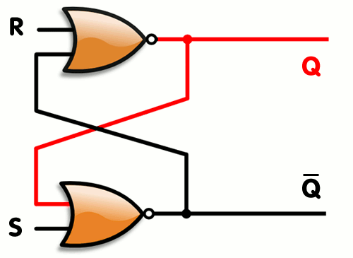
Both the S and the R inputs of the previous SR bistable have now been replaced by two inputs called the J and K inputs, respectively after its inventor Jack Kilby. Then this equates to: J = S and K = R.

The two 2-input AND gates of the gated SR bistable have now been replaced by two 3-input NAND gates with the third input of each gate connected to the outputs at Q and Q. This cross coupling of the SR flip-flop allows the previously invalid condition of S = “1” and R = “1” state to be used to produce a “toggle action” as the two inputs are now interlocked.

If the circuit is now “SET” the J input is inhibited by the “0” status of Q through the lower NAND gate. If the circuit is “RESET” the K input is inhibited by the “0” status of Q through the upper NAND gate. As Q and Q are always different we can use them to control the input. When both inputs J and K are equal to logic “1”, the JK flip flop toggles as shown in the following truth table.


The Truth Table for the JK Function

same as
for the
SR Latch
Input Output Description
J K Q Q
0 0 0 0 Memory
no change
0 0 0 1
0 1 1 0 Reset Q » 0
0 1 0 1
1 0 0 1 Set Q » 1
1 0 1 0
toggle
action
1 1 0 1 Toggle
1 1 1 0

Then the JK flip-flop is basically an SR flip flop with feedback which enables only one of its two input terminals, either SET or RESET to be active at any one time thereby eliminating the invalid condition seen previously in the SR flip flop circuit. Also when both the J and the K inputs are at logic level “1” at the same time, and the clock input is pulsed either “HIGH”, the circuit will “toggle” from its SET state to a RESET state, or visa-versa. This results in the JK flip flop acting more like a T-type toggle flip-flop when both terminals are “HIGH”.

Although this circuit is an improvement on the clocked SR flip-flop it still suffers from timing problems called “race” if the output Q changes state before the timing pulse of the clock input has time to go “OFF”. To avoid this the timing pulse period ( T ) must be kept as short as possible (high frequency). As this is sometimes not possible with modern TTL IC’s the much improved Master-Slave JK Flip-flop was developed.

The master-slave flip-flop eliminates all the timing problems by using two SR flip-flops connected together in a series configuration. One flip-flop acts as the “Master” circuit, which triggers on the leading edge of the clock pulse while the other acts as the “Slave” circuit, which triggers on the falling edge of the clock pulse. This results in the two sections, the master section and the slave section being enabled during opposite half-cycles of the clock signal.

The TTL 74LS73 is a Dual JK flip-flop IC, which contains two individual JK type bistable’s within a single chip enabling single or master-slave toggle flip-flops to be made. Other JK flip flop IC’s include the 74LS107 Dual JK flip-flop with clear, the 74LS109 Dual positive-edge triggered JK flip flop and the 74LS112 Dual negative-edge triggered flip-flop with both preset and clear inputs.


Dual JK Flip-flop 74LS73

74ls73 dual jk flip flop


The Master-Slave JK Flip-flop

The Master-Slave Flip-Flop is basically two gated SR flip-flops connected together in a series configuration with the slave having an inverted clock pulse. The outputs from Q and Q from the “Slave” flip-flop are fed back to the inputs of the “Master” with the outputs of the “Master” flip flop being connected to the two inputs of the “Slave” flip flop. This feedback configuration from the slave’s output to the master’s input gives the characteristic toggle of the JK flip flop as shown below.


The Master-Slave JK Flip Flop

master slave jk flip flop

The input signals J and K are connected to the gated “master” SR flip flop which “locks” the input condition while the clock (Clk) input is “HIGH” at logic level “1”. As the clock input of the “slave” flip flop is the inverse (complement) of the “master” clock input, the “slave” SR flip flop does not toggle. The outputs from the “master” flip flop are only “seen” by the gated “slave” flip flop when the clock input goes “LOW” to logic level “0”.

When the clock is “LOW”, the outputs from the “master” flip flop are latched and any additional changes to its inputs are ignored. The gated “slave” flip flop now responds to the state of its inputs passed over by the “master” section.

Then on the “Low-to-High” transition of the clock pulse the inputs of the “master” flip flop are fed through to the gated inputs of the “slave” flip flop and on the “High-to-Low” transition the same inputs are reflected on the output of the “slave” making this type of flip flop edge or pulse-triggered.

Then, the circuit accepts input data when the clock signal is “HIGH”, and passes the data to the output on the falling-edge of the clock signal. In other words, the Master-Slave JK Flip flop is a “Synchronous” device as it only passes data with the timing of the clock signal.

In the next tutorial about Sequential Logic Circuits, we will look at Multivibrators that are used as waveform generators to produce the clock signals to switch sequential circuits.


Source: http://www.electronics-tutorials.ws/sequential/seq_2.html

D flip-flop


The D-type Flip Flop

One of the main disadvantages of the basic SR NAND Gate bistable circuit is that the indeterminate input condition of “SET” = logic “0” and “RESET” = logic “0” is forbidden. This state will force both outputs to be at logic “1”, over-riding the feedback latching action and whichever input goes to logic level “1” first will lose control, while the other input still at logic “0” controls the resulting state of the latch.

But in order to prevent this from happening an inverter can be connected between the “SET” and the “RESET” inputs to produce another type of flip flop circuit known as a Data Latch, Delay flip flop, D-type Bistable, D-type Flip Flop or just simply a D Flip Flop as it is more generally called.

The D Flip Flop is by far the most important of the Clocked Flip-flops as it ensures that ensures that inputs S and R are never equal to one at the same time. The D-type flip flop are constructed from a gated SR flip-flop with an inverter added between the S and the R inputs to allow for a single D (data) input.

Then this single data input, labelled D, is used in place of the “set” signal, and the inverter is used to generate the complementary “reset” input thereby making a level-sensitive D-type flip-flop from a level-sensitive RS-latch as now S = D and R = not D as shown.


D-type Flip-Flop Circuit

d-type flip flop

We remember that a simple SR flip-flop requires two inputs, one to “SET” the output and one to “RESET” the output. By connecting an inverter (NOT gate) to the SR flip-flop we can “SET” and “RESET” the flip-flop using just one input as now the two input signals are complements of each other. This complement avoids the ambiguity inherent in the SR latch when both inputs are LOW, since that state is no longer possible.

Thus this single input is called the “DATA” input. If this data input is held HIGH the flip flop would be “SET” and when it is LOW the flip flop would change and become “RESET”. However, this would be rather pointless since the flip flop’s output would always change on every pulse applied to this data input.

To avoid this an additional input called the “CLOCK” or “ENABLE” input is used to isolate the data input from the flip flop’s latching circuitry after the desired data has been stored. The effect is that D input condition is only copied to the output Q when the clock input is active. This then forms the basis of another sequential device called a D Flip Flop.

The “D flip flop” will store and output whatever logic level is applied to its data terminal so long as the clock input is HIGH. Once the clock input goes LOW the “set” and “reset” inputs of the flip-flop are both held at logic level “1” so it will not change state and store whatever data was present on its output before the clock transition occurred. In other words the output is “latched” at either logic “0” or logic “1”.


Truth Table for the D-type Flip Flop

Clk D Q Q Description
↓ » 0 X Q Q Memory
no change
↑ » 1 0 0 1 Reset Q » 0
↑ » 1 1 1 0 Set Q » 1

Note that: and indicates direction of clock pulse as it is assumed D-type flip flops are edge triggered


The Master-Slave D Flip Flop

The basic D-type flip flop can be improved further by adding a second SR flip-flop to its output that is activated on the complementary clock signal to produce a “Master-Slave D-type flip flop”. On the leading edge of the clock signal (LOW-to-HIGH) the first stage, the “master” latches the input condition at D, while the output stage is deactivated.

On the trailing edge of the clock signal (HIGH-to-LOW) the second “slave” stage is now activated, latching on to the output from the first master circuit. Then the output stage appears to be triggered on the negative edge of the clock pulse. “Master-Slave D-type flip flops” can be constructed by the cascading together of two latches with opposite clock phases as shown.


The Master-Slave D Flip Flop Circuit

master slave d-type flip flop circuit

We can see from above that on the leading edge of the clock pulse the master flip-flop will be loading data from the data D input, therefore the master is “ON”. With the trailing edge of the clock pulse the slave flip-flop is loading data, i.e. the slave is “ON”. Then there will always be one flip-flop “ON” and the other “OFF” but never both the master and slave “ON” at the same time. Therefore, the output Q acquires the value of D, only when one complete pulse, ie, 0-1-0 is applied to the clock input.

There are many different D flip-flop IC’s available in both TTL and CMOS packages with the more common being the 74LS74 which is a Dual D flip-flop IC, which contains two individual D type bistable’s within a single chip enabling single or master-slave toggle flip-flops to be made. Other D flip-flop IC’s include the 74LS174 HEX D flip-flop with direct clear input, the 74LS175 Quad D flip-flop with complementary outputs and the 74LS273 Octal D-type flip flop containing eight D-type flip flops with a clear input in one single package.


74LS74 Dual D-type Flip Flop

74ls74 d flip flop


Using The D-type Flip Flop For Frequency Division

One main use of a D-type flip flop is as a Frequency Divider. If the Q output on a D-type flip-flop is connected directly to the D input giving the device closed loop “feedback”, successive clock pulses will make the bistable “toggle” once every two clock cycles.

In the counters tutorials we saw how the Data Latch can be used as a “Binary Divider”, or a “Frequency Divider” to produce a “divide-by-2″ counter circuit, that is, the output has half the frequency of the clock pulses. By placing a feedback loop around the D-type flip flop another type of flip-flop circuit can be constructed called a T-type flip-flop or more commonly a T-type bistable, that can be used as a divide-by-two circuit in binary counters as shown below.


Divide-by-2 Counter

divide by 2 counter

It can be seen from the frequency waveforms above, that by “feeding back” the output from Q to the input terminal D, the output pulses at Q have a frequency that are exactly one half ( ƒ/2 ) that of the input clock frequency, ( ƒIN ). In other words the circuit produces frequency division as it now divides the input frequency by a factor of two (an octave) as Q = 1 once every two clock cycles.


D Flip Flops as Data Latches

As well as frequency division, another useful application of the D flip flop is as a Data Latch. A data latch can be used as a device to hold or remember the data present on its data input, thereby acting a bit like a single bit memory device and IC’s such as the TTL 74LS74 or the CMOS 4042 are available in Quad format exactly for this purpose. By connecting together four, 1-bit data latches so that all their clock inputs are connected together and are “clocked” at the same time, a simple “4-bit” Data latch can be made as shown below.


4-bit Data Latch

4-bit data latch


Transparent Data Latch

The Data Latch is a very useful device in electronic and computer circuits. They can be designed to have very high output impedance at both outputs Q and its inverse or complement output Q to reduce the impedance effect on the connecting circuit when used as a buffer, I/O port, bi-directional bus driver or even a display driver.

But a single “1-bit” data latch is not very practical to use on its own and instead commercially available IC’s incorporate 4, 8, 10, 16 or even 32 individual data latches into one single IC package, and one such IC device is the 74LS373 Octal D-type transparent latch.

The eight individual data latches or bistables of the 74LS373 are “transparent” D-type flip-flops, meaning that when the clock (CLK) input is HIGH at logic level “1”, (but can also be active low) the outputs at Q follows the data D inputs.

In this configuration the latch is said to be “open” and the path from D input to Q output appears to be “transparent” as the data flows through it unimpeded, hence the name transparent latch.

When the clock signal is LOW at logic level “0”, the latch “closes” and the output at Q is latched at the last value of the data that was present before the clock signal changed and no longer changes in response to D.


8-bit Data Latch

8 bit data latch
Functional diagram of the 74LS373 Octal Transparent Latch


The D-type Flip Flop Summary

The data or D-type Flip Flop can be built using a pair of back-to-back SR latches and connecting an inverter (NOT Gate) between the S and the R inputs to allow for a single D (data) input. The basic D flip flop circuit can be improved further by adding a second SR flip-flop to its output that is activated on the complementary clock signal to produce a “Master-Slave D flip-flop” device.

The difference between a D-type latch and a D-type flip-flop is that a latch does not have a clock signal to change state whereas a flip-flop always does. The D flip-flop is an edge triggered device which transfers input data to Q on clock rising or falling edge. Data Latches are level sensitive devices such as the data latch and the transparent latch.

In the next tutorial about Sequential Logic Circuits, we will look at connecting together data latches to produce another type of sequential logic circuit called a Shift Register that are used to convert parallel data into serial data and vice versa.


Source: http://www.electronics-tutorials.ws/sequential/seq_4.html

Sunday, September 7, 2014

SR flip-flop


Sequential Logic Basics

Unlike Combinational Logic circuits that change state depending upon the actual signals being applied to their inputs at that time, Sequential Logic circuits have some form of inherent “Memory” built in to them as they are able to take into account their previous input state as well as those actually present, a sort of  ”before” and “after” effect is involved with sequential logic circuits.

In other words, the output state of a “sequential logic circuit” is a function of the following three states, the “present input”, the “past input” and/or the “past output”. Sequential Logic circuits remember these conditions and stay fixed in their current state until the next clock signal changes one of the states, giving sequential logic circuits “Memory”.

Sequential logic circuits are generally termed as two state or Bistable devices which can have their output or outputs set in one of two basic states, a logic level “1” or a logic level “0” and will remain “latched” (hence the name latch) indefinitely in this current state or condition until some other input trigger pulse or signal is applied which will cause the bistable to change its state once again.

Sequential Logic Representation

sequential logic representation
 

The word “Sequential” means that things happen in a “sequence”, one after another and in Sequential Logic circuits, the actual clock signal determines when things will happen next. Simple sequential logic circuits can be constructed from standard Bistable circuits such as: Flip-flops, Latches and Counters and which themselves can be made by simply connecting together universal NAND Gates and/or NOR Gates in a particular combinational way to produce the required sequential circuit.


 Classification of Sequential Logic

As standard logic gates are the building blocks of combinational circuits, bistable latches and flip-flops are the basic building blocks of Sequential Logic Circuits. Sequential logic circuits can be constructed to produce either simple edge-triggered flip-flops or more complex sequential circuits such as storage registers, shift registers, memory devices or counters. Either way sequential logic circuits can be divided into the following three main categories:

1. Event Driven – asynchronous circuits that change state immediately when enabled.

 2. Clock Driven – synchronous circuits that are synchronised to a specific clock signal. 

3. Pulse Driven – which is a combination of the two that responds to triggering pulses.

sequential logic device
 
As well as the two logic states mentioned above logic level “1” and logic level “0”, a third element is introduced that separates sequential logic circuits from their combinational logic counterparts, namely TIME. Sequential logic circuits return back to their original steady state once reset and sequential circuits with loops or feedback paths are said to be “cyclic” in nature.


We now know that in sequential circuits changes occur only on the application of a clock signal making it synchronous, otherwise the circuit is asynchronous and depends upon an external input. To retain their current state, sequential circuits rely on feedback and this occurs when a fraction of the output is fed back to the input and this is demonstrated as:


 Sequential Feedback Loop

sequential feedback loop
 

The two inverters or NOT gates are connected in series with the output at Q fed back to the input. Unfortunately, this configuration never changes state because the output will always be the same, either a “1” or a “0”, it is permanently set. However, we can see how feedback works by examining the most basic sequential logic components, called the SR flip-flop.

SR Flip-Flop

The SR flip-flop, also known as a SR Latch, can be considered as one of the most basic sequential logic circuit possible. This simple flip-flop is basically a one-bit memory bistable device that has two inputs, one which will “SET” the device (meaning the output = “1”), and is labelled S and another which will “RESET” the device (meaning the output = “0”), labelled R.

Then the SR description stands for “Set-Reset”. The reset input resets the flip-flop back to its original state with an output Q that will be either at a logic level “1” or logic “0” depending upon this set/reset condition.

A basic NAND gate SR flip-flop circuit provides feedback from both of its outputs back to its opposing inputs and is commonly used in memory circuits to store a single data bit. Then the SR flip-flop actually has three inputs, Set, Reset and its current output Q relating to it’s current state or history. The term “Flip-flop” relates to the actual operation of the device, as it can be “flipped” into one logic Set state or “flopped” back into the opposing logic Reset state.


The NAND Gate SR Flip-Flop

The simplest way to make any basic single bit set-reset SR flip-flop is to connect together a pair of cross-coupled 2-input NAND gates as shown, to form a Set-Reset Bistable also known as an active LOW SR NAND Gate Latch, so that there is feedback from each output to one of the other NAND gate inputs. This device consists of two inputs, one called the Set, S and the other called the Reset, R with two corresponding outputs Q and its inverse or complement Q (not-Q) as shown below.

The Basic SR Flip-flop

sr flip flop


The Set State

Consider the circuit shown above. If the input R is at logic level “0” (R = 0) and input S is at logic level “1” (S = 1), the NAND gate Y has at least one of its inputs at logic “0” therefore, its output Q must be at a logic level “1” (NAND Gate principles). Output Q is also fed back to input “A” and so both inputs to NAND gate X are at logic level “1”, and therefore its output Q must be at logic level “0”.

Again NAND gate principals. If the reset input R changes state, and goes HIGH to logic “1” with S remaining HIGH also at logic level “1”, NAND gate Y inputs are now R = “1” and B = “0”. Since one of its inputs is still at logic level “0” the output at Q still remains HIGH at logic level “1” and there is no change of state. Therefore, the flip-flop circuit is said to be “Latched” or “Set” with Q = “1” and Q = “0”.


 Reset State

In this second stable state, Q is at logic level “0”, (not Q = “0”) its inverse output at Q is at logic level “1”, (Q = “1”), and is given by R = “1” and S = “0”. As gate X has one of its inputs at logic “0” its output Q must equal logic level “1” (again NAND gate principles). Output Q is fed back to input “B”, so both inputs to NAND gate Y are at logic “1”, therefore, Q = “0”.

If the set input, S now changes state to logic “1” with input R remaining at logic “1”, output Q still remains LOW at logic level “0” and there is no change of state. Therefore, the flip-flop circuits “Reset” state has also been latched and we can define this “set/reset” action in the following truth table.


 Truth Table for this Set-Reset Function

State S R Q Q Description
Set 1 0 0 1 Set Q » 1
1 1 0 1 no change
Reset 0 1 1 0 Reset Q » 0
1 1 1 0 no change
Invalid 0 0 1 1 Invalid Condition

It can be seen that when both inputs S = “1” and R = “1” the outputs Q and Q can be at either logic level “1” or “0”, depending upon the state of the inputs S or R BEFORE this input condition existed. Therefore the condition of S = R = “1” does not change the state of the outputs Q and Q.

However, the input state of S = “0” and R = “0” is an undesirable or invalid condition and must be avoided. The condition of S = R = “0” causes both outputs Q and Q to be HIGH together at logic level “1” when we would normally want Q to be the inverse of Q. The result is that the flip-flop looses control of Q and Q, and if the two inputs are now switched “HIGH” again after this condition to logic “1”, the flip-flop becomes unstable and switches to an unknown data state based upon the unbalance as shown in the following switching diagram.


 S-R Flip-flop Switching Diagram

sr flip flop switching diagram

This unbalance can cause one of the outputs to switch faster than the other resulting in the flip-flop switching to one state or the other which may not be the required state and data corruption will exist. This unstable condition is generally known as its Meta-stable state.

Then, a bistable SR flip-flop or SR latch is activated or set by a logic “1” applied to its S input and deactivated or reset by a logic “1” applied to its R. The SR flip-flop is said to be in an “invalid” condition (Meta-stable) if both the set and reset inputs are activated simultaneously.

As well as using NAND gates, it is also possible to construct simple one-bit SR Flip-flops using two cross-coupled NOR gates connected in the same configuration. The circuit will work in a similar way to the NAND gate circuit above, except that the inputs are active HIGH and the invalid condition exists when both its inputs are at logic level “1”, and this is shown below.


 The NOR Gate SR Flip-flop

nor gate sr flip flop


Switch Debounce Circuits

Edge-triggered flip-flops require a nice clean signal transition, and one practical use of this type of set-reset circuit is as a latch used to help eliminate mechanical switch “bounce”. As its name implies, switch bounce occurs when the contacts of any mechanically operated switch, push-button or keypad are operated and the internal switch contacts do not fully close cleanly, but bounce together first before closing (or opening) when the switch is pressed.

 This gives rise to a series of individual pulses which can be as long as tens of milliseconds that an electronic system or circuit such as a digital counter may see as a series of logic pulses instead of one long single pulse and behave incorrectly. For example, during this bounce period the output voltage can fluctuate wildly and may register multiple input counts instead of one single count. Then set-reset SR Flip-flops or Bistable Latch circuits can be used to eliminate this kind of problem and this is demonstrated below.


SR Flip Flop Switch Debounce Circuit

sr flip flop switch debounce circuit

Depending upon the current state of the output, if the set or reset buttons are depressed the output will change over in the manner described above and any additional unwanted inputs (bounces) from the mechanical action of the switch will have no effect on the output at Q.

When the other button is pressed, the very first contact will cause the latch to change state, but any additional mechanical switch bounces will also have no effect. The SR flip-flop can then be RESET automatically after a short period of time, for example 0.5 seconds, so as to register any additional and intentional repeat inputs from the same switch contacts, such as multiple inputs from a keyboards “RETURN” key.

Commonly available IC’s specifically made to overcome the problem of switch bounce are the MAX6816, single input, MAX6817, dual input and the MAX6818 octal input switch debouncer IC’s. These chips contain the necessary flip-flop circuitry to provide clean interfacing of mechanical switches to digital systems.

Set-Reset bistable latches can also be used as Monostable (one-shot) pulse generators to generate a single output pulse, either high or low, of some specified width or time period for timing or control purposes. The 74LS279 is a Quad SR Bistable Latch IC, which contains four individual NAND type bistable’s within a single chip enabling switch debounce or monostable/astable clock circuits to be easily constructed.

Quad SR Bistable Latch 74LS279

74ls279 quad sr latch


Gated or Clocked SR Flip-Flop

It is sometimes desirable in sequential logic circuits to have a bistable SR flip-flop that only changes state when certain conditions are met regardless of the condition of either the Set or the Reset inputs. By connecting a 2-input AND gate in series with each input terminal of the SR Flip-flop a Gated SR Flip-flop can be created. This extra conditional input is called an “Enable” input and is given the prefix of “EN“. The addition of this input means that the output at Q only changes state when it is HIGH and can therefore be used as a clock (CLK) input making it level-sensitive as shown below.


Gated SR Flip-flop

gated sr flip flop

When the Enable input “EN” is at logic level “0”, the outputs of the two AND gates are also at logic level “0”, (AND Gate principles) regardless of the condition of the two inputs S and R, latching the two outputs Q and Q into their last known state. When the enable input “EN” changes to logic level “1” the circuit responds as a normal SR bistable flip-flop with the two AND gates becoming transparent to the Set and Reset signals.

This additional enable input can also be connected to a clock timing signal (CLK) adding clock synchronisation to the flip-flop creating what is sometimes called a “Clocked SR Flip-flop“. So a Gated Bistable SR Flip-flop operates as a standard bistable latch but the outputs are only activated when a logic “1” is applied to its EN input and deactivated by a logic “0”.

In the next tutorial about Sequential Logic Circuits, we will look at another type of simple edge-triggered flip-flop which is very similar to the RS flip-flop called a JK Flip-flop named after its inventor, Jack Kilby. The JK flip-flop is the most widely used of all the flip-flop designs as it is considered to be a universal device.


JS1701 Project - RTL SR-Latch Flipflop

Flip flops are a crucial part of digital logic.  These sequential-logic circuits provide a way to memorize state; or more often referred to as 'memory'.  They are the building blocks of types of RAM that all computers have used for years.  Today, I wanted to build a simple SR-Latch flipflop.  Here's a look at the internal structure from Wikipedia:


By cross-coupling two NOR gates, we end up with the ability to 'set' and 'reset' the circuit.  Producing a 1 'set' or a 0 'reset'.  Notice that instead of the NOR gates having two external inputs, they only really have one.  The other crosses over to the output of the other gate.

By using RTL logic, I can easily construct this circuit using only 4 resistors, and 2 transistors:


This of course, could be simplified by only taking up 3 rows of the breadboard per latch.  Although this is pretty convenient, SR-Latches are not as useful as gated-latches which I will get into later.  For now, I have been able to prove this circuit works in the following video:

Once again, the input / output of the circuit clutters up the breadboard.  However, this has been rigged to give you a simple example of a working circuit.  The green LED represents the value of 1 or 'set'.  The red LED likewise represents 0 or 'reset'.  The push-buttons are simply completing the circuit to the base of the transistor, causing it to saturate and thus 'step' the circuit to the respective state.


Source: http://www.electronics-tutorials.ws/sequential/seq_1.html
             http://www.thestarrlab.com/2014/07/js1701-project-rtl-sr-latch-flipflop.html